
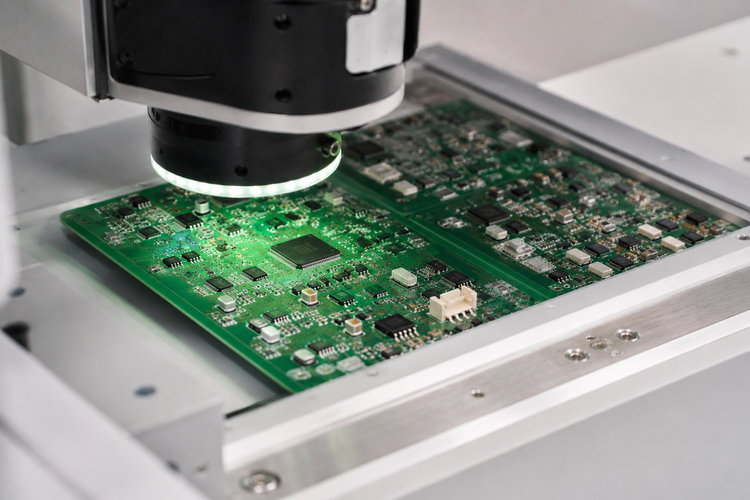
Design for AOI means laying out a PCB so automated optical inspection can read the board correctly after SMT assembly.
AOI is useful, but it is not magic. It compares the assembled board against programmed inspection rules, reference images, CAD data, and expected visual features. If the layout makes those features hard to see, the AOI machine will complain. Sometimes it is right. Sometimes it is just offended by your footprint.
False failures slow down production because every flagged board needs review, rework judgment, or operator confirmation. For startups, that means longer NPI cycles, noisier quality data, and more friction with the contract manufacturer. To understand where AOI fits beside solder paste inspection, see Titoma’s guide on AOI vs SPI in SMT manufacturing.
AOI is not just a checkbox after reflow. Research from Michigan Technological University on AOI-based PCB fault detection points to the same basic reason manufacturers use it: PCB density keeps rising, and visual inspection needs image processing to find defects early without slowing every build into manual review. The catch is simple. If the layout gives the camera poor visual information, the AOI result gets noisy.
What Does Design for AOI Mean?
Design for AOI means making PCB layout choices that let the inspection system clearly see component presence, position, polarity, solder condition, and visible defects.
AOI systems use cameras, controlled lighting, image processing, and programmed rules to inspect assembled boards. Titoma’s overview of what AOI means in electronics manufacturing explains the basic inspection concept, but the short version is simple: the machine can only judge what it can see. If a polarity mark sits under a tall connector, or if a silkscreen label runs into a pad, the AOI program starts guessing. Guessing is not a quality system.
AOI works best when the PCB layout, component library, assembly drawing, centroid file, BOM, and acceptable quality criteria tell the same story. This is why AOI belongs inside the DFM discussion, not after the first build already has fifty nuisance calls per panel.
| AOI Goal | Layout Helps When | Layout Hurts When |
|---|---|---|
| Check component presence | Parts have clear outlines and visible bodies | Parts are hidden by neighboring tall components |
| Check orientation | Pin 1 and polarity marks are visible after assembly | Marks are missing, covered, or inconsistent |
| Check solder joints | Pads have inspectable toe, heel, and side fillets | Pads are crowded by silkscreen, copper, or adjacent parts |
| Reduce false calls | Footprints, markings, and spacing are consistent | Every similar part uses a slightly different layout style |
For a practical electronics team, design for AOI is not about pleasing the machine. It is about keeping inspection useful enough that operators trust it. Once operators stop trusting AOI, it becomes expensive theater with blinking lights.
How Does Component Placement Affect AOI Accuracy?
Component placement affects AOI accuracy because cameras need a clear viewing angle around each part, especially for polarity, solder joints, and package edges.
Dense placement saves board area, but it can make inspection harder. AOI needs enough visual access to identify whether a part is shifted, rotated, missing, tombstoned, or poorly soldered. When small passives sit too close to connectors, shields, inductors, or electrolytic capacitors, the taller part can block the camera view or cast shadows.
Orientation also matters. If identical diodes, LEDs, ICs, and polarized capacitors face different directions across the board without a good reason, AOI programming becomes more complex. The CM can still program it, but you just paid someone to manage avoidable variation.
| Placement Choice | Effect on AOI | Better Layout Practice |
|---|---|---|
| Very tight spacing between small passives | Higher risk of false bridge, skew, or missing-part calls | Use the CM’s minimum placement spacing, not just CAD clearance |
| Tall parts beside low-profile components | Camera shadowing and blocked solder joint view | Keep inspection-critical parts away from tall components where possible |
| Mixed orientation for similar polarized parts | More AOI programming work and higher review risk | Standardize orientation when routing and function allow it |
| Components placed close to board edge | Handling rails or clamps may block inspection | Respect board edge clearance and panel rail requirements |
Startups often push density because the enclosure is already too small, the antenna wants space, the battery wants space, and reality has poor customer service. That is normal. But the CM should review critical placement before layout freeze, especially around fine-pitch ICs, BGAs, LEDs, connectors, and test points.
Why Do Polarity Marks Matter for AOI?
Polarity marks matter because AOI needs a visible reference to confirm that polarized components are installed in the correct direction.
For diodes, LEDs, ICs, tantalum capacitors, and electrolytic capacitors, the board should show clear polarity or pin 1 information that matches the assembly drawing and component datasheet. Do not assume the package body marking is enough. Some markings are faint, reflective, inconsistent by supplier, or hidden after placement.
| Part Type | AOI Risk | Layout Check |
|---|---|---|
| LED | Wrong orientation may pass visual review if package marking is unclear | Use consistent cathode or anode marking on silkscreen and assembly drawing |
| Diode | Body stripe may be hard to read under lighting glare | Place a visible diode symbol or polarity marker outside the pads |
| IC | Pin 1 dot may be hidden or low contrast | Add a clear pin 1 indicator on silkscreen or assembly layer |
| Polarized capacitor | Marking conventions can differ by capacitor type | Make positive or negative marking explicit and consistent |
The best rule is boring: one marking convention, used everywhere, checked against the BOM and assembly drawing. Boring is underrated in manufacturing.
How Do Pad Design and Silkscreen Choices Affect AOI Programming?
Pad design and silkscreen choices affect AOI programming because they change how clearly the machine can identify solder joints, part outlines, and reference marks.
AOI does not inspect the schematic. It inspects the physical board. Pad geometry, solder mask openings, silkscreen placement, and copper exposure all influence what the camera sees. A footprint that is electrically correct can still be annoying to inspect if the visible solder area is too small or visually inconsistent.
Use IPC land pattern guidance and your CM’s process rules when creating footprints. IPC design training references standards such as IPC-2221 for printed board design and other design documentation standards, while IPC-A-610 provides visual acceptability criteria for assembled boards. The point is not to worship standards. The point is to avoid inventing footprint art at 2 a.m.
| Layout Feature | Good for AOI | Bad for AOI |
|---|---|---|
| Pad size | Matches package and CM assembly capability | Too small to show consistent solder fillet |
| Pad spacing | Enough gap to distinguish joints and bridges | Fine spacing with no process discussion |
| Solder mask | Clear mask definition around pads | Mask slivers or unclear exposed copper areas |
| Silkscreen | Outside pads, readable after assembly | Printed over pads, under parts, or too close to solder areas |
Silkscreen is useful when it supports inspection. It becomes a problem when reference designators, outlines, or polarity marks overlap pads or disappear under components. Keep markings readable but out of the solderable area. This also helps manual inspection and rework, which still happen more often than PowerPoint claims.
What Silkscreen Choices Help AOI?
Silkscreen helps AOI when it gives clear component outlines, polarity references, and readable designators without interfering with solder joints.
For small parts, prioritize polarity and orientation over decorative outlines. For ICs, show pin 1 clearly. For connectors, show orientation and mating direction if there is any realistic chance of confusion. Do not place critical information under the body of the component. Hidden markings are not documentation. They are archaeology.
| Silkscreen Item | Use It For | Avoid |
|---|---|---|
| Reference designator | Manual review, debug, and rework | Text so small it becomes white dust |
| Pin 1 mark | IC orientation and AOI reference | Placing it under the package body |
| Polarity mark | LED, diode, capacitor direction | Mixing positive and negative conventions without notes |
| Component outline | Part placement review | Lines crossing pads or solder mask openings |
If silkscreen space is limited, put the most critical markings on the assembly drawing and fabrication notes too. AOI programming often uses CAD and centroid data, but human review still benefits from clear board-level cues.
How Do Panelization and Board Edge Clearance Affect Inline AOI?
Panelization and board edge clearance affect inline AOI because the machine, conveyor, clamps, fiducials, and camera path all need predictable access to the board.
Inline AOI is part of the SMT production flow. The panel moves through conveyors, stops in a fixed position, and gets inspected by cameras under controlled lighting. If the panel has poor edge clearance, weak rails, missing fiducials, or inconsistent orientation, inspection setup becomes harder and less repeatable.
This is not only a contract manufacturing issue. RIT’s Center for Electronics Manufacturing and Assembly uses AOI equipment to inspect PCB assemblies where transistors and other components must be aligned accurately. That is the practical point: AOI depends on repeatable placement, clear visual features, and board layouts that do not hide the defects you want to catch.
This is where PCB design meets factory handling. A board can pass electrical DRC and still be awkward to run through SMT. Titoma’s broader PCB DFM checklist covers this same production reality: layout choices affect whether boards flow through the line smoothly, not just whether they look nice in CAD.
| Panel Feature | Why AOI Cares | Practical Rule |
|---|---|---|
| Panel fiducials | Help AOI align the inspection program to the physical panel | Use clear global fiducials on the panel and local fiducials for fine-pitch areas when needed |
| Board edge clearance | Prevents rails, clamps, or tooling from blocking parts | Keep components away from edges based on the CM’s conveyor and tooling rules |
| Panel rails | Support transport through stencil printing, placement, reflow, and AOI | Add rails when the board shape or component placement needs handling support |
| Panel orientation | Affects programming, inspection flow, and review consistency | Keep orientation consistent unless there is a strong assembly reason not to |
Fiducials deserve special attention. Place them where the AOI system can see them clearly, with proper clearance from solder mask, copper, silkscreen, and components. Local fiducials near fine-pitch components can help with placement and inspection accuracy, especially when tolerances are tight.
What Board Edge Mistakes Cause AOI Problems?
Board edge mistakes cause AOI problems when components, fiducials, or inspection targets sit too close to the conveyor handling area.
Small boards often need panel rails because the SMT line needs something stable to grip. If you place components close to the final board edge without discussing panelization, the CM may need to add rails, rotate the board, change breakaway tab locations, or block part of the inspection view.
| Board Edge Issue | Production Result | Better DFM Choice |
|---|---|---|
| Components too close to edge | Conveyor or fixture interference | Confirm edge keepout with the CM before release |
| Fiducials near routed edge | Unstable alignment or poor recognition | Place fiducials on stable areas with clean clearance |
| Tabs near sensitive components | Depanelization stress or inspection obstruction | Keep tabs away from fragile parts and fine-pitch areas |
| Irregular board outline | More custom handling and inspection setup | Use panel rails and tooling holes where needed |
Panelization is not just a fabrication detail. It affects stencil printing, pick-and-place stability, reflow handling, AOI alignment, depanelization, and sometimes test fixtures. Treat it like part of the product, because the factory certainly will.
What PCB Layout Decisions Cause AOI False Failures?
AOI false failures usually come from layout choices that make good assemblies look visually inconsistent or hard to classify.
A false failure does not always mean the AOI program is bad. Sometimes the design gives the system poor visual evidence. Reflection, shadowing, inconsistent footprints, tight component spacing, unclear polarity marks, and silkscreen interference can all trigger calls that operators must review manually.
False failures matter because they pollute yield data. If AOI reports too many nuisance defects, the team spends time sorting noise from real defects. That makes it harder to detect actual process drift, such as solder paste issues, placement offsets, or reflow problems. For upstream context, Titoma’s article on common SPI defects in SMT manufacturing shows how inspection earlier in the line can catch solder paste problems before AOI has to deal with the results.
| Layout Decision | Possible AOI False Failure | Why It Happens |
|---|---|---|
| Uneven pad geometry on similar parts | False solder volume or alignment calls | The AOI system sees different visual patterns for the same expected joint |
| Silkscreen close to pads | False bridge or contamination calls | White ink near solder areas can confuse image thresholds |
| Missing polarity marks | False orientation calls or missed wrong-orientation defects | The system lacks a clear visual reference |
| Reflective metal parts near inspection areas | False missing, skew, or solder calls | Lighting reflection changes the captured image |
| Parts crowded around tall components | False insufficient solder or missing-part calls | Shadows and blocked camera angles reduce inspection confidence |
The fix is not always more spacing. Sometimes the board has no room. The practical fix is to know which areas are inspection-critical and discuss them early with the CM. Fine-pitch ICs, polarized parts, small passives near connectors, LEDs, shields, and high-reliability solder joints deserve extra attention.
What Should You Share With Your CM at the DFM Stage?
You should share the full PCB data package, component information, inspection expectations, and known layout constraints with your CM before the design is frozen.
Do not send only Gerbers and expect the CM to reverse-engineer your intent. AOI setup depends on accurate CAD data, centroid files, BOM details, polarity conventions, assembly drawings, panel requirements, and quality criteria. If your files disagree, the AOI program becomes a detective story. Those are fun on Netflix, less fun during production ramp.
For data transfer, Gerbers still show up everywhere, but richer formats can reduce interpretation errors. The IPC-2581 Consortium describes IPC-DPMX, also known as IPC-2581, as an open standard for PCB design and manufacturing data exchange. That matters because AOI setup depends on clean component, pad, layer, and assembly data, not just copper artwork.
At the DFM stage, ask the CM how their AOI system handles your package types, board finish, panel format, fiducials, minimum spacing, and polarity markings. This fits naturally into a broader DFM, DFA, and DFX review, where manufacturability, assembly, testing, and inspection get checked together instead of treated as separate silos.
| File or Information | Why the CM Needs It | AOI Impact |
|---|---|---|
| Gerber and drill files | Define copper, solder mask, silkscreen, and board geometry | Helps verify visible inspection features and clearances |
| ODB++ or IPC-2581 data | Provides richer manufacturing data than Gerbers alone | Can reduce setup errors in CAM and inspection programming |
| Centroid file | Defines component locations and rotations | Critical for AOI component position and orientation checks |
| BOM with manufacturer part numbers | Identifies exact package, body style, and markings | Helps AOI account for real component appearance |
| Assembly drawing | Shows orientation, polarity, special notes, and build options | Reduces ambiguity during AOI programming and review |
| Quality class or acceptance criteria | Defines what level of workmanship is acceptable | Aligns AOI thresholds with product risk and customer requirements |
Also share any special cases. If a component has alternate approved suppliers with different body markings, say so. If a footprint supports multiple package variants, say so. If a part is mechanically blocked from clear inspection, say so before the build, not after AOI starts shouting.
Design for AOI Checklist Before Sending Files
A good design for AOI checklist confirms that inspection-critical features are visible, consistent, and aligned with the CM’s SMT process.
This checklist will not replace a CM review, but it will make that review faster and less painful. It also gives hardware teams a simple way to catch layout issues before they become production noise.
| Check | What to Confirm | Why It Matters |
|---|---|---|
| Component spacing | AOI can see part edges and solder joints | Reduces false missing, skew, and solder calls |
| Polarity marks | Pin 1 and polarity are visible after assembly | Helps catch wrong-orientation defects |
| Footprint consistency | Similar parts use consistent land patterns | Makes AOI programming more stable |
| Silkscreen clearance | Ink does not overlap pads or solderable areas | Prevents visual confusion near solder joints |
| Fiducials | Global and local fiducials have proper clearance | Improves alignment for placement and inspection |
| Panelization | Rails, tabs, and edge clearance fit the SMT line | Prevents handling and camera access issues |
| Data package | BOM, centroid, assembly drawing, and PCB files agree | Reduces AOI setup errors and review delays |
The best time to reduce AOI false failures is before layout release. Once the board is already in SMT, every preventable false call becomes operator time, engineering review, and schedule drag.
Final Takeaway
Design for AOI is part of PCB design for manufacturing, not a separate inspection task added at the end.
AOI can catch real SMT defects, but only when the PCB gives the machine clear visual evidence. Component spacing, orientation, pad geometry, silkscreen, fiducials, panel rails, and documentation all affect whether AOI improves quality or creates noise.
For startups, the practical move is simple: involve the CM before the design freeze, share complete manufacturing data, and ask what their AOI system needs to inspect your board reliably. The layout may still be tight. The product may still be hard. But at least the inspection system will not fail boards just because the design made good parts look suspicious.