

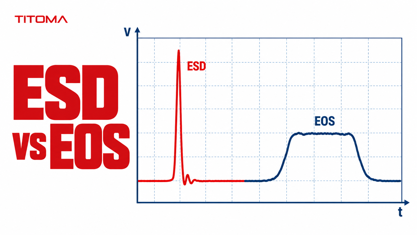
ESD (Electrostatic Discharge) is a high-voltage, nanosecond-scale discharge caused by static electricity. EOS (Electrical Overstress) is a longer, higher-current event caused by exceeding a component’s voltage or current rating from any source, not just static. Both can damage or destroy electronic components, but they require different prevention strategies.
ESD vs EOS at a Glance
| Factor | ESD | EOS |
|---|---|---|
| Duration | Nanoseconds to microseconds | Milliseconds to seconds |
| Voltage | Very high and can reach kilovolts | Often lower, but sustained |
| Cause | Static electricity buildup and discharge | Any voltage or current beyond rated specification |
| Typical damage pattern | Localized, often at a single junction or input | Broader thermal damage that can affect multiple structures |
| Primary prevention | Grounding, ESD-safe handling, and ionization | Component derating, circuit protection, and controlled power sequencing |
What Makes ESD Different From EOS?
The important difference is the waveform and the source of the energy. ESD begins with charge accumulated on a person, a tool, a cable, a device, or an insulating material. When it finds a path, it discharges extremely quickly. The voltage can be dramatic, but the event has limited duration.
EOS is what happens when voltage, current, or power stays beyond a component’s limit long enough to do damage. It may come from a supply overshoot, a wiring fault, an inductive load switching off, an incorrect test setup, a hot-plug event, or bad power-up sequencing. The electrical stress need not look impressive on a bench. A few volts above an absolute maximum rating, applied long enough, can be sufficient.
That distinction affects the physical evidence. ESD may damage an I/O protection structure, a gate oxide, or one junction while leaving little visible evidence. EOS has more time to deposit energy. It can melt bond wires, burn metal traces, crack a package, or short several nodes. Those are tendencies, not a diagnosis from a photograph. A failed IC rarely leaves a signed confession.
RS DesignSpark’s comparison of EOS and ESD makes the same useful point: EOS is defined by a component limit being exceeded, whether the result is immediate damage, malfunction, or a shortened lifetime.
Why Are They Often Confused in Failure Analysis?
In the broadest engineering sense, ESD is one kind of electrical overstress. A discharge puts voltage and current beyond what a device can tolerate. In factory and field practice, however, teams separate ESD and EOS because the prevention paths are different. Treating every electrically damaged component as “EOS/ESD” creates a tidy label and an unhelpful corrective action.
Consider a board that fails only after a cable is connected. The cause may be a static discharge from the user, but it may also be a supply transient, a ground-potential difference, or an external signal that rises before the device supply. A wrist strap audit cannot resolve the latter. Likewise, a TVS diode on an external connector does not protect a loose IC being handled at a rework bench.
Failure signatures overlap. Both mechanisms can create leakage, shifted parameters, opens, shorts, or latent reliability loss. The component’s internal ESD clamp can also be harmed by a sustained EOS event. The clamp was designed to conduct briefly, not serve as a power supply regulator.
Good analysis starts with context: where the failure appeared, whether it is linked to assembly, test, power cycling, cable connection, or field use, and whether the failure repeats. Then it compares the electrical history with the schematic, layout, data-sheet limits, and any available transient captures. Infineon’s EOS guidance for an over-voltage input pin is a practical reminder that exceeding an absolute maximum rating can leave a pin open or shorted, with the exact result depending on the event.
Do You Need Protection Against Both?
Yes. ESD-safe manufacturing is necessary, but it protects the handling environment. It does not prove that a finished product survives a bad power sequence, an inductive kick, or a supply cable plugged in with the wrong reference. EOS protection is a circuit and system responsibility that continues after the product has left the factory.
| Risk point | ESD control | EOS control |
|---|---|---|
| Assembly and rework | Grounded operators, dissipative work areas, approved trays and packaging | Powered test fixtures with current limits and verified connections |
| External ports | Connector-level ESD path and controlled handling | TVS devices, series impedance, filtering, and correct grounding layout |
| Power input | Handling controls for unpowered boards | Fuses, current limiting, surge protection, reverse-polarity protection, and derating |
| Startup and shutdown | Usually not the primary control | Sequencing, discharge paths, reset strategy, and validation across corner cases |
Protection must match the product’s environment. A sealed battery device with no external cable has different threats from an industrial controller connected to long wiring and motors. Component data sheets set absolute maximum ratings, but a design should not live at those limits. Derating gives tolerance for normal variation and for the unpleasant things a customer can do with a connector.
Verification also needs both views. An ESD program checks personnel grounding, mats, tools, and packaging. Product validation checks power-up, power-down, short-circuit behavior, reverse polarity where relevant, hot-plugging, loaded outputs, and transient exposure. Tests should follow the use case rather than a generic checklist pasted onto every product.
EVT, DVT, and PVT testing provide useful gates for exposing these issues before mass production. A power-sequencing weakness that is invisible on a calm lab bench can become a warranty problem once several suppliers, cables, and operating temperatures are involved.
How This Affects Your Manufacturing Partner Selection
Ask an EMS or ODM partner what happens when an assembled board fails electrically. “We follow ESD procedures” is only half an answer. It describes prevention on the line, not whether the team can distinguish a static-handling event from an overstress caused by the circuit, fixture, or application.
- Ask for the ESD control program and evidence of operator, workstation, and packaging verification.
- Ask how failed boards are quarantined and preserved so rework does not erase evidence.
- Ask whether the failure analysis process reviews schematic limits, power sequencing, test-fixture behavior, and connector events.
- Ask what measurements they can capture before removing a failed component: supply waveforms, inrush current, pin voltage, continuity, and thermal evidence.
- Ask how corrective actions are separated into process controls, design changes, test-fixture changes, and supplier actions.
- Ask whether they validate the proposed fix on new builds rather than closing a report after a visual inspection.
Automated optical inspection is valuable for visible assembly defects, but it cannot determine why an IC’s internal protection structure failed. It belongs in the evidence chain, alongside electrical test, process records, and waveform data.
At Titoma, a failure report is tied back to the build history, design information, and test conditions so a suspected ESD or EOS issue produces a specific next step. That may be an ESD control correction, a fixture fix, or a circuit change. It should never be a reflexive label followed by crossed fingers.
When evidence is incomplete, the right engineering conclusion may be “electrical damage pending further analysis.” That still moves the work forward: it preserves suspect parts, directs the next measurement, and stops a factory from changing the wrong process. Fast containment is sensible. A confident but unsupported root cause is expensive.
FAQs
Can an ESD-safe factory still produce EOS failures?
How can you tell whether a failed IC suffered ESD or EOS?
Does an ESD protection diode prevent electrical overstress?
