

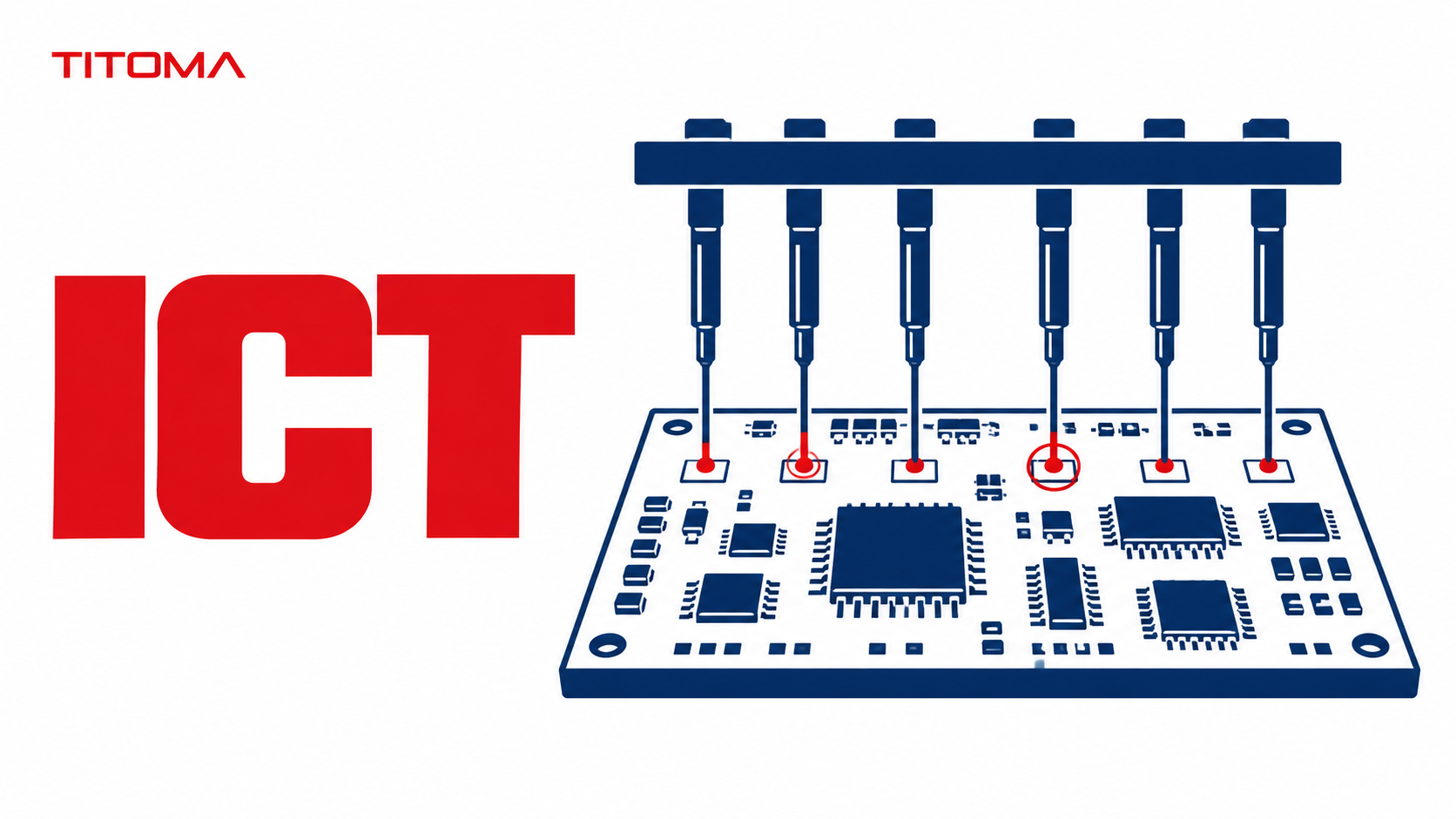
ICT (In-Circuit Test) is a PCB assembly test method that uses probes to check individual components and electrical connections on a populated board. It can find many assembly defects, including shorts, opens, and wrong components. ICT does not prove that the finished product works as intended or that its firmware behaves correctly.
What Does ICT Stand For?
ICT stands for In-Circuit Test, sometimes called in-circuit testing. The test examines a printed circuit board assembly after components have been soldered, rather than testing loose parts or judging the board only by appearance.
Each test probe contacts a designed test point, component lead, connector pin, or other accessible net. The tester applies a stimulus and measures the response. Depending on the test program and access available, it can verify resistance, capacitance, diode polarity, continuity, and whether a component is present or connected to the expected net.
That makes ICT particularly useful for catching repeatable PCBA process errors before boards reach a later test station. It is a coverage tool, not a promise that every possible fault has been found. The distinction matters when a quote simply says “100% tested” and leaves the actual test method unspecified.
How Does In-Circuit Testing Work?
Traditional ICT uses a bed-of-nails fixture. The fixture contains spring-loaded probes positioned for the board’s test points and holds the assembly in a repeatable location. When the board is pressed into the fixture, many nets can be contacted at once. A test system runs a programmed sequence of measurements, usually in seconds.
A flying-probe tester moves a small number of probes to each point under software control. It avoids the cost and lead time of a dedicated fixture, which makes it useful for prototypes and lower-volume builds. Its cycle time is usually longer because it makes contacts sequentially.
| Test approach | Bed-of-nails ICT | Flying-probe test |
|---|---|---|
| Probe contact | Many fixed probes contact the board together | Movable probes visit points in sequence |
| Fixture | Dedicated fixture is required | No dedicated bed-of-nails fixture |
| Typical fit | Stable, higher-volume production | Prototypes, revisions, and lower volumes |
| Cycle time | Usually short once the fixture is ready | Usually longer per board |
| Main tradeoff | Fixture NRE and test-point access | Lower setup cost but slower throughput |
Good ICT starts before the tester is powered on. The design, fixture, test program, and assembly process need to agree on what can actually be reached and measured. The IPC standards body publishes design and test guidance because test coverage is a design decision as much as a factory decision.
What Defects Can ICT Catch?
ICT is strongest where an electrical measurement can distinguish a good assembly from a bad one. It often catches a large share of assembly defects, especially on boards with adequate test access and a well-maintained test program.
| Defect | How ICT can identify it | Practical limitation |
|---|---|---|
| Short circuit | Measures unexpectedly low resistance or continuity between nets | Detection depends on the nets being accessible and isolated enough to measure |
| Open circuit | Checks for missing continuity through a trace, solder joint, or connector path | Parallel paths can make an open harder to isolate |
| Wrong or missing component | Measures a value outside the programmed tolerance or detects an absent response | Some parts cannot be measured accurately in circuit without special techniques |
| Incorrect orientation | Checks diode, LED, transistor, or polarized capacitor behavior and polarity | Coverage varies with access and circuit topology |
| Solder defect | Finds an electrical open, short, or unexpected value caused by a poor joint | It does not visually describe the solder joint itself |
For visible assembly problems, AOI can inspect solder paste, component placement, polarity marks, and solder joints without electrical contact. AOI and ICT overlap in a few cases, but they answer different questions. A board can look correctly assembled and still have an electrical fault; it can also pass an electrical check while a visual workmanship issue deserves attention.
What Can’t ICT Catch?
ICT does not run the product through its real operating use case. It normally cannot confirm that firmware boots, communications protocols work across a full system, power rails remain stable under dynamic load, or an analogue circuit meets every performance requirement in its application.
That gap is exactly what FCT is built to close. Functional testing powers the board and checks behaviour at the product level. The right split between ICT and functional test depends on the product, failure risks, and production volume. Treating either one as a substitute for the other is how boards move forward with a blind spot already built into the test plan.
ICT also has limited reach into dense packages. It may verify accessible nets around a BGA, but it cannot directly inspect every hidden solder ball. X-ray, boundary scan, process controls, and functional tests can supplement that gap. Boundary scan is based on IEEE 1149.1 and can provide test access where physical probing is limited, provided the devices and design support it.
What Does ICT Require From Your PCB Design?
ICT needs accessible, documented points on the nets that matter. Test pads must be large enough for reliable contact, placed where fixture probes can reach them, and kept clear of tall parts, shields, and mechanical features. A test point that is technically on the PCB but impossible to contact in a fixture is not useful test coverage.
Designers also need to consider test-point spacing, probe force, board support, connector access, and which circuits can be measured without damaging a sensitive device or being distorted by parallel paths. This work is usually called design for test, or DFT. It belongs alongside design for manufacturing early in the layout and review process.
Late additions are awkward. Adding test pads can require a layout revision, move components, alter impedance-controlled routing, or conflict with the enclosure. Once a fixture has been built, a small PCB change may also require fixture rework and a revised test program. These are ordinary production costs, but they are cheaper when identified before the design is frozen.
Test strategy should also change as the product matures. A prototype may justify flying probe and hands-on debugging. A stable production build may justify a fixture and faster automated coverage. The test plan should sit alongside the build gates in EVT, DVT, and PVT, rather than being treated as a final factory detail.
How to Know If Your Manufacturing Partner Does Proper ICT?
“We have ICT” is not enough information to judge coverage. Ask which tester and fixture approach they plan to use, whether the board has been reviewed for test access, and which nets and component types will be measured. A meaningful answer includes known exclusions, not only a claim that the board will be tested.
- Ask for the planned ICT coverage or a coverage report, including nets and components that cannot be tested.
- Ask whether the fixture is dedicated, who owns it, what changes trigger rework, and how it will be maintained.
- Ask how failed boards are diagnosed, logged, repaired, and retested rather than simply rejected.
- Ask how ICT results connect to AOI, functional test, and traceability data for the same serialised board.
- Ask what faults are deliberately left for another method, especially firmware, high-speed interfaces, RF, and load-dependent behaviour.
At Titoma, the practical work is to review test access with the design and production teams before fixtures and volume commitments make a change expensive. The aim is not to force every net into ICT. It is to document the coverage, pair it with the tests the product needs, and make the remaining limits visible to the buyer.
