

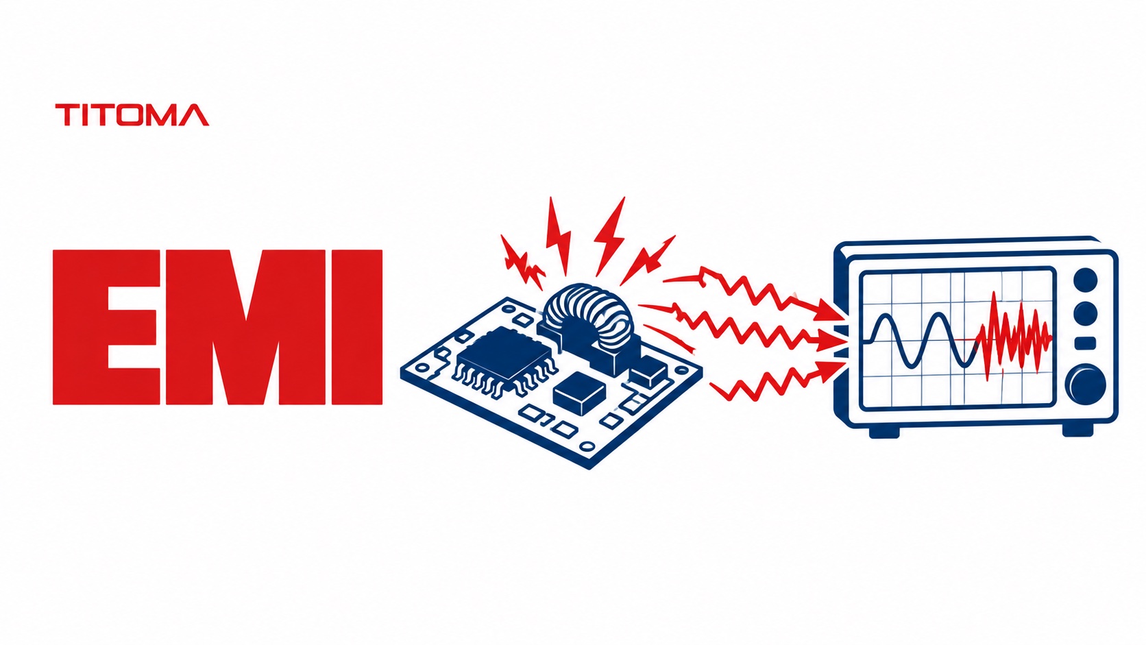
Electromagnetic interference (EMI) is unwanted electromagnetic energy that disrupts the normal operation of an electronic circuit or device. It travels through cables and power lines as conducted noise or through the air as radiated energy. EMI matters because excessive emissions can cause failures, trigger resets, and prevent products from passing FCC Part 15 or CE electromagnetic compatibility tests.
What Does EMI Stand For in Electronics?
EMI stands for electromagnetic interference. In electronics, it describes electrical noise that one circuit creates and another circuit, cable, radio, sensor, or device receives.
A product can create EMI internally, pick it up from its environment, or do both. A switch-mode power supply may create noise that couples into a nearby sensor. A long USB cable may carry noise away from a PCB and become an efficient antenna. A motor may disturb a microcontroller enough to cause a reset.
EMI is closely related to electromagnetic compatibility, or EMC. EMI describes the unwanted energy itself. EMC asks whether the complete product can operate acceptably in its electromagnetic environment without causing unacceptable interference to other equipment.
What Causes Electromagnetic Interference?
Most EMI starts with changing current or voltage. The faster the transition and the larger the current loop or conductive path, the more likely it is to create emissions. A circuit does not need a radio transmitter to cause a problem.
- Switch-mode power supplies: Buck, boost, flyback, and other converters switch current quickly. Their high-current loops and switch nodes can produce broadband noise.
- High-speed clocks and digital edges: A 25 MHz clock does not only create energy at 25 MHz. Fast edge rates also create harmonics at much higher frequencies.
- Poor return paths: A signal trace crossing a split ground plane forces return current to take a longer route, increasing loop area and radiation.
- Motors, relays, and inductive loads: Brushed motors, solenoids, relays, and long load wiring can create switching transients and common-mode noise.
- Long cables and connectors: USB, Ethernet, mains, display, sensor, and motor cables can carry common-mode current and radiate it well beyond the PCB.
The bench can be misleading. A prototype may appear stable with a short test cable, a quiet power supply, and no final enclosure. Add the production cable harness, mains adapter, plastic housing, display, or motor load and the emissions picture changes quickly.
Conducted vs Radiated EMI: What’s the Difference?
| Factor | Conducted EMI | Radiated EMI |
|---|---|---|
| Travel path | Moves through power, signal, or data cables | Travels through the air as electromagnetic fields |
| Typical concern | Noise returning through mains, DC input, or cable connections | Energy emitted by PCB traces, switching loops, clocks, and cables |
| How it is measured | Sampled from a defined cable or supply connection with a test network | Measured with an antenna at a controlled test distance |
| Typical fixes | Input filtering, common-mode chokes, capacitor placement, cable filtering | Smaller current loops, continuous ground planes, shielding, enclosure and cable changes |
Conducted and radiated EMI often have the same root cause. A poorly contained switching-current loop can inject noise into the input cable, which then radiates. Treating only the cable may reduce one test result while leaving the underlying layout issue in place.
The FCC’s Part 15 measurement guidance distinguishes procedures for intentional and unintentional radiators. The applicable method depends on the product and rule path, so a lab should confirm the test plan before final samples are built.
How Does EMI Affect a Product?
EMI can be an emissions problem, an immunity problem, or both. Emissions are the noise the product sends out. Immunity is the product’s ability to keep working when noise arrives from somewhere else.
At product level, EMI can show up as data errors, touch-screen glitches, false sensor readings, audio noise, wireless dropouts, MCU resets, or unstable power rails. In industrial equipment, it may cause a safety interlock or communication bus to misbehave. In a consumer device, it may simply make the product look unreliable.
It also affects market access. A product that exceeds applicable limits may fail testing needed for FCC Certification or CE marking. The failure itself is rarely the expensive part. The expensive part is discovering that the PCB, enclosure, or cable arrangement must change after prototype hardware, tooling, and a lab booking are already in place.
Electrostatic discharge is related but different. Electrostatic discharge is a sudden transfer of charge, such as a person touching a connector. It can inject a large transient into a product, while EMI covers a broader range of unwanted electromagnetic energy and coupling paths.
How Do You Reduce EMI in PCB Design?
Good EMI performance begins before the PCB is routed. Component selection matters, but layout and mechanical decisions decide whether noise stays contained or finds a path into the rest of the product.
- Use a layer stack-up with a continuous reference plane under high-speed signals. This gives return current a short, predictable path.
- Keep high di/dt loops small, especially around switching regulators, input capacitors, inductors, and power switches.
- Place decoupling capacitors close to the relevant IC supply pins, with short connections to power and ground.
- Keep noisy power stages away from sensitive analogue, RF, and sensor circuitry while maintaining controlled return paths.
- Filter at connectors where cables leave the PCB, and decide early whether common-mode chokes, ferrites, or TVS devices are needed.
- Design the enclosure and cable routing as part of the system. Shield termination, connector position, and seams can materially change emissions.
Texas Instruments’ EMI layout guidance for buck regulators highlights two common priorities: reduce high transient-current loop area and reduce the exposed area of high transient-voltage nodes. These are ordinary layout decisions, but they have a large effect on test results.
This is why EMI belongs in design for manufacturing. PCB stack-up, component placement, connector selection, enclosure geometry, and cable routing are easier to correct before fabrication and tooling. Once production parts exist, even a small change can require a new build and another test cycle.
How Do You Know If Your Manufacturing Partner Can Help With EMI?
Ask about EMI before sending Gerbers for release. A capable partner should identify the product features that create risk, review the layout and mechanical design, prepare representative lab samples, and control changes after testing.
- Ask whether the team performs EMI-focused layout review before the PCB is released.
- Ask how it handles pre-compliance scans, lab coordination, test sample configuration, and test-failure investigation.
- Ask how the factory controls substitutions to antennas, inductors, power supplies, cables, shielding materials, and enclosure parts after test approval.
- Ask who keeps the test reports, released BOM, labeling files, and production configuration records.
At Titoma, EMI risk is considered during design review and manufacturing preparation, when PCB, enclosure, and cable decisions can still be changed without disrupting production. The goal is not to promise that every product passes first time. It is to avoid treating a compliance-lab failure as the first EMI review the product receives.
